All-rounder nanoparticles: Perovskites in next-generation solar cells, X-ray detectors, and light‑emitting devices
- LAC
- D-CHAB
- Highlights
The group of Prof. Kovalenko lays the foundation for next-generation optoelectric devices by using perovskite nanocrystals
Perovskites
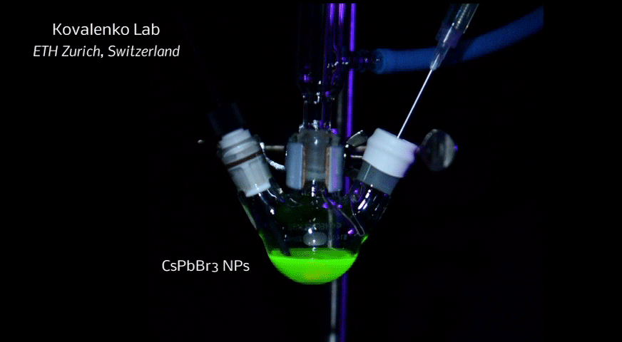
Lead halide perovskites are the new center of attention in the materials research, because they are able to convert light into electrical signal and vice versa. Now researchers in the group of Prof. Kovalenko are successfully developing perovskites for new applications. They have produced tiny crystals of these materials (nanocrystals) that open new avenues in this field of research. We are on the verge of the next generation of inexpensive yet highly efficient light-emitting diodes (LEDs) and television displays, X-ray detectors, and lasers.
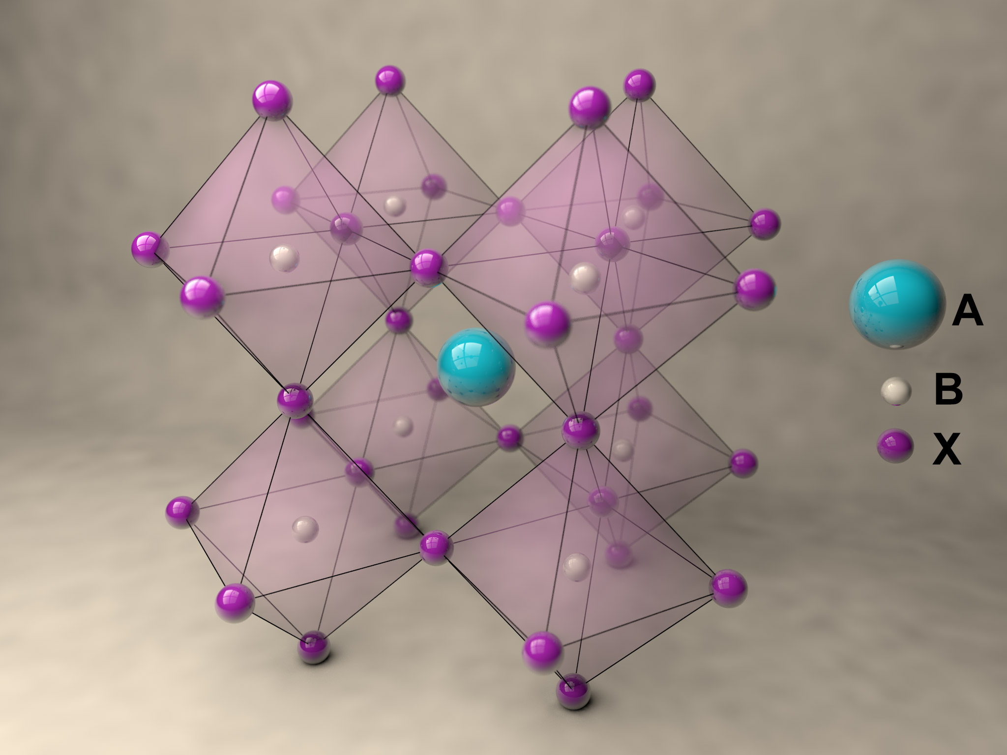
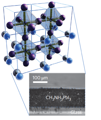
Perovskites are inorganic or mixed organic-inorganic compounds that have the same crystal structure as the mineral perovskite which is also known as calcium titanate, CaTiO3. They are named after their discoverer, the Russian mineralogist Lev Perovski who discovered the mineral in the 19th century in the Ural Mountains.
Light Emitters
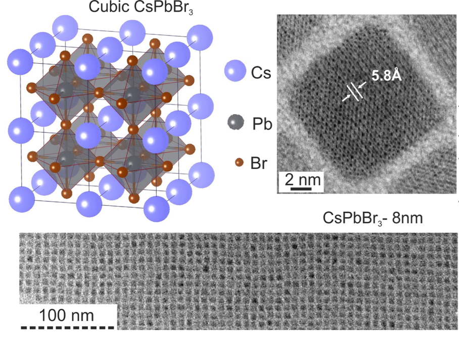
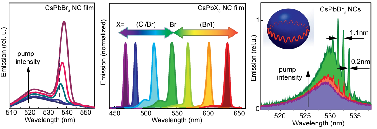
A new fascinating aspect beyond light-to-current conversion used in CH3NH3PbI3-based solar cells is the ability of perovskites to emit bright light in various well-defined colors.[1] These so-called semiconductor nanocrystals, also known as quantum dots, can be utilized in color displays as well as in new, highly efficient LEDs. The all-inorganic perovskites CsPbX3 (X= Cl, Br, I, or mixtures thereof) can be easily synthesized in the form of cubic nanocrystals emitting different colors depending on their size and composition. The latter aspect – facile composition tuning of emission color – differentiates them from predecessor quantum dot materials such as cadmium chalcogenides that rely mainly on quantum-size-effects. The key properties are the high luminescence quantum yields of up to 90%, narrow emission linewidths providing pure colors and the coverage of a wide color spectrum. Especially in blue and green regions, these nanocrystals clearly outperform their Cd-chalcogenide-based cousins.
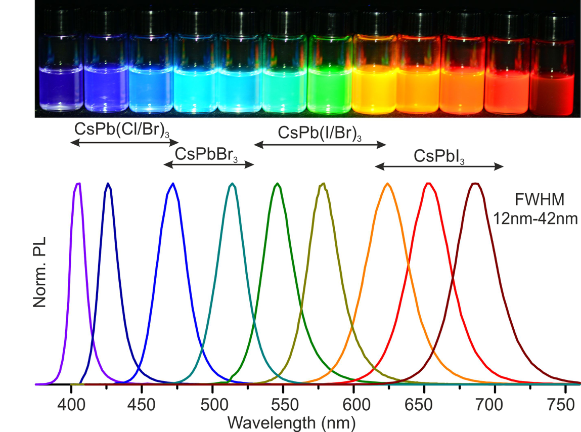
In order to yield different colors, another finding was made by Kovalenko and his coworkers in a recent study [2]: Instead of synthesizing each nanocube of a distinct size and color separately, the perovskite nanocrystals can easily be converted into each other by quickly exchanging their anions (for example, by replacing bromide with iodide), thus adjusting their emission color post-synthetically (see animation below). This method can also be used to produce otherwise inaccessible or hard to synthesize morphologies of nanocrystals.
X-ray Detectors
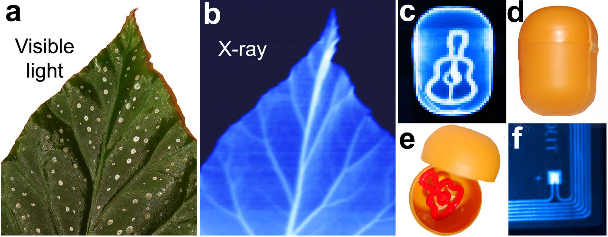
Among the main advantages of perovskite semiconductors are their low cost of production as well as the solution-based processability. A new study[3] shows that the ability of perovskite nanocrystals to convert sunlight into electrical current can be transferred to the highly sensitive detection of X-rays as e.g. used in medical diagnostic devices. The performance of this new generation of perovskite-based X-ray detectors is comparable with current solid-state technology used in a wide range of X-ray applications. Established X‑ray detectors are fabricated from silicon or selenium by intricate and expensive vacuum processing. Perovskites in contrast can be spray-coated or inkjet printed in order to form a uniform semiconducting film suitable for highly responsive detectors.
In order to capture an X-ray image of bones in the body, the X-rays are focused onto the affected area. Depending on the tissue, they are absorbed or they pass through, eventually reaching a detector. The detector has to be able to efficiently absorb the radiation in order to produce a well-resolved image. The lead and iodine atoms of the perovskites are the heavy atoms suitable for this task. With the ability to produce cheap X-ray sensors that are on par with established solid-state detectors, many new fields of application can be entered: inexpensive large-area detectors could simply be spray-coated or inkjet-printed even onto flexible materials, extending the work of material sciences to be able to radiograph larger or more complex objects.
Towards nanocrystal lasers
Excellent light emission properties of CsPbX3 perovskites inspired the researchers to investigate stimulated emission from the films of these materials, thus to evaluate and the prosepcts for inexpensive nanocrystal lasers[4]. They could show that coated onto silica microspheres that act as optical resonators, the perovskites exhibit low thresholds for lasing. Furthermore, perovskite nanocrystals could be excited without a resonator sphere to exhibit so-called “random lasing”. This can be used, for instance, in cryptography where random number generation is vital for scrambling or encoding sensitive data.
[1] L. Protesescu, S. Yakunin, M.I. Bodnarchuk, F. Krieg, R. Caputo, C. Holman Hendon, R.X. Yang, A. Walsh, and M.V. Kovalenko. external pageNanocrystals of Cesium Lead Halide Perovskites (CsPbX3, X=Cl, Br, and I): Novel Optoelectronic Materials Showing Bright Emission with Wide Color Gamut. Nano Letters, 2015, 15, 3692–3696.
[2] G. Nedelcu, L. Protesescu, S. Yakunin, M. I. Bodnarchuk, M. Grotevent and M. V. Kovalenko. external pageFast anion-exchange in highly luminescent nanocrystals of cesium lead halide perovskites (CsPbX3, X=Cl, Br, I). Nano Letters, 2015, 15, 5635–5640.
[3] S. Yakunin, M. Sytnyk, D. Kriegner, S. Shrestha, M. Richter, G. J. Matt, H. Azimi, Ch. J. Brabec, J. Stangl, M. V. Kovalenko and W. Heiss. external pageDetection of X-ray photons by solution-processed lead halide perovskites. Nature Photonics, 2015, 9, 444 - 449.
[4] S. Yakunin, L. Protesescu, F. Krieg, M. I. Bodnarchuk, G. Nedelcu, M. Humer, G. De Luca, M. Fiebig, W. Heiss, and M. V. Kovalenko. external pageLow-threshold amplified spontaneous emission and lasing from colloidal nanocrystals of cesium lead halide perovskites CsPbX3 (X=Cl, Br, I). Nature Communications, 2015, 6, 8056